Phone: +86-752-3198333
Email: sales@xcpcb.net
Website: en.xcpcb.net
Address: South of Lianfa Avenue, Yongqiao Industrial Park, Zhongkai High-tech Zone, Huizhou, Guangdong Province
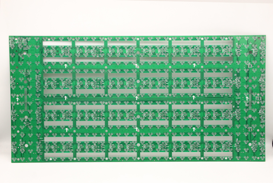
The deformation of PCB board needs to be studied several aspects such as material, structure, pattern distribution, processing process, etc. This article will analyze explain the various causes improvement methods that may cause deformation.

First, the area of copper plating on the circuit board is uneven, which will worsen the board bending board warping.
Generally, a large area of copper foil is designed on the circuit board for grounding. Sometimes the Vcc layer is also designed with a large area of copper foil. When these large areas of copper foil cannot be evenly distributed on the same circuit board When you go up, it will cause the problem of uneven heat absorption heat dissipation speed. Of course, the circuit board will also expand contract. If the expansion contraction cannot be caused at the same time, it will cause different stresses deformation. The upper limit of the Tg value, the board will begin to soften, causing permanent deformation.
Second, the connection points (vias) of the layers on the circuit board will limit the board's expansion contraction
Today's circuit boards are mostly multi-layer boards, there are rivet-like connection points between layers. The connection points are divided into through holes, blind holes buried holes. there are connection points, the board is restricted. The effect of expansion contraction will also cause plate bending plate warping indirectly. The weight of the circuit board itself will cause the board to sag deform
Generally, reflow furnaces use a chain to drive the circuit board in the reflow furnace. That is, the two sides of the board are used as fulcrum points to support the entire board. Because of its own amount, it will show the phenomenon of middle depression, resulting in plate bending.
Third, the depth of V-Cut the connection bar will affect the amount of deformation of the puzzle
Basically, V-Cut is the culprit that destroys the structure of the board. Because V-Cut is to cut grooves in the original large sheet, the V-Cut is prone to deformation. pcb customization
Relevant webpage materials related resources on this site are sourced the Internet. If there is any infringement, please inform us quickly. We will delete it within 24 hours!