Phone: +86-752-3198333
Email: sales@xcpcb.net
Website: en.xcpcb.net
Address: South of Lianfa Avenue, Yongqiao Industrial Park, Zhongkai High-tech Zone, Huizhou, Guangdong Province
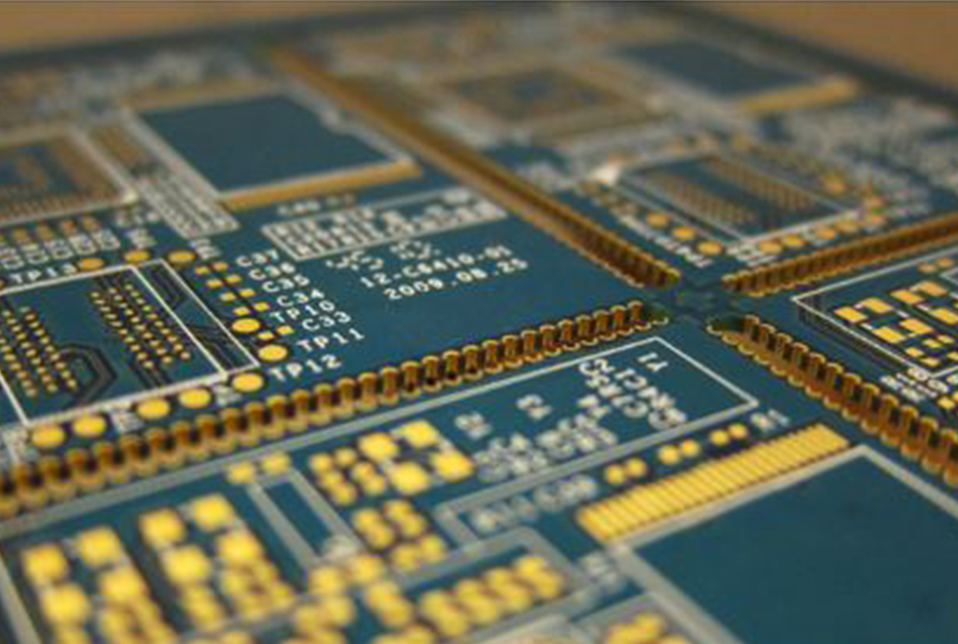
When designing the PCB board, the most consideration for wiring is how to connect the various layers to the network signal lines. The denser the high-speed PCB board lines, the higher the density of vias (VIA), the vias can play to each layer. The role of electrical connections. Multi-layer circuit board PCB proofing often receives feedback the board factory that "holes are too close to the line, which exceeds the process capability." So, if the vias are too close, will it be difficult to produce will it affect product reliability?

1. Two holes too close will affect the aging of PCB drilling process. When the first hole is drilled after drilling the second hole, the material in one side is too thin, the drill bit is uniformly stressed the drill bit is heat-dissipated, which will cause the drill bit to break, which will cause the PCB hole to collapse be unsightly. The hole is conducting.
2. The vias in the multilayer board will have an eyelet ring on each layer of the circuit, the surrounding environment of the eyelet ring of each layer will be pinned unpinned, the environment will be different. When the wire is too close the hole is too close, when the CAM engineer of the PCB board factory optimizes the file, the hole ring will be cut away to ensure a safe distance (3mil) the solder ring to the copper / wire of different networks.
3. The hole position tolerance of the drilled hole is ≤0.05mm. When the tolerance is at the upper limit, the following conditions will occur in the multilayer board.
(1) When the lines are dense, the small gaps between the vias other elements 360 ° appear irregularly. To ensure a safe distance of 3mil, the pads may appear multi-directionally cut PAD.
(2) According to the data of the source file, the hole edge to line edge is 6mil, the hole ring is 4mil, the ring to line is only 2mil. To ensure that there is a 3mil safety distance between the ring the line, the 1mil solder ring needs to be cut, the pad after cutting is only 3mil . When the tolerance deviation of the hole position is the upper limit of 0.05mm (2mil), the hole ring has only 1mil left.
4. PCB production will produce a small amount of deviation in the same direction, the direction of the pad being cut is irregular, in the worst case, individual holes will be broken.
5. The influence of lamination deviation in multilayer boards. Taking a six-layer board as an example, two core boards + copper foil are laminated to form a six-layer board. During the pressing process, there may be a deviation of ≤0.05mm when the core plate 1 the core plate 2 are pressed together, the inner layer holes will also have an irregular deviation of 360 ° after the pressing.
To sum up, the drilling process affects the PCB yield PCB production efficiency. There is no complete copper protection around the small hole of the ring, the PCB open short test can pass. There is no problem in the early use of the product, but the long-term reliability is enough. Double-sided multilayer circuit board
Relevant webpage materials related resources on this site are sourced the Internet. If there is any infringement, please inform us quickly. We will delete it within 24 hours!